- 您现在的位置:买卖IC网 > Sheet目录510 > SI4705-D-EVB (Silicon Laboratories Inc)BOARD EVAL MOBILE SI4704/05-D50
Si4704/05-D50
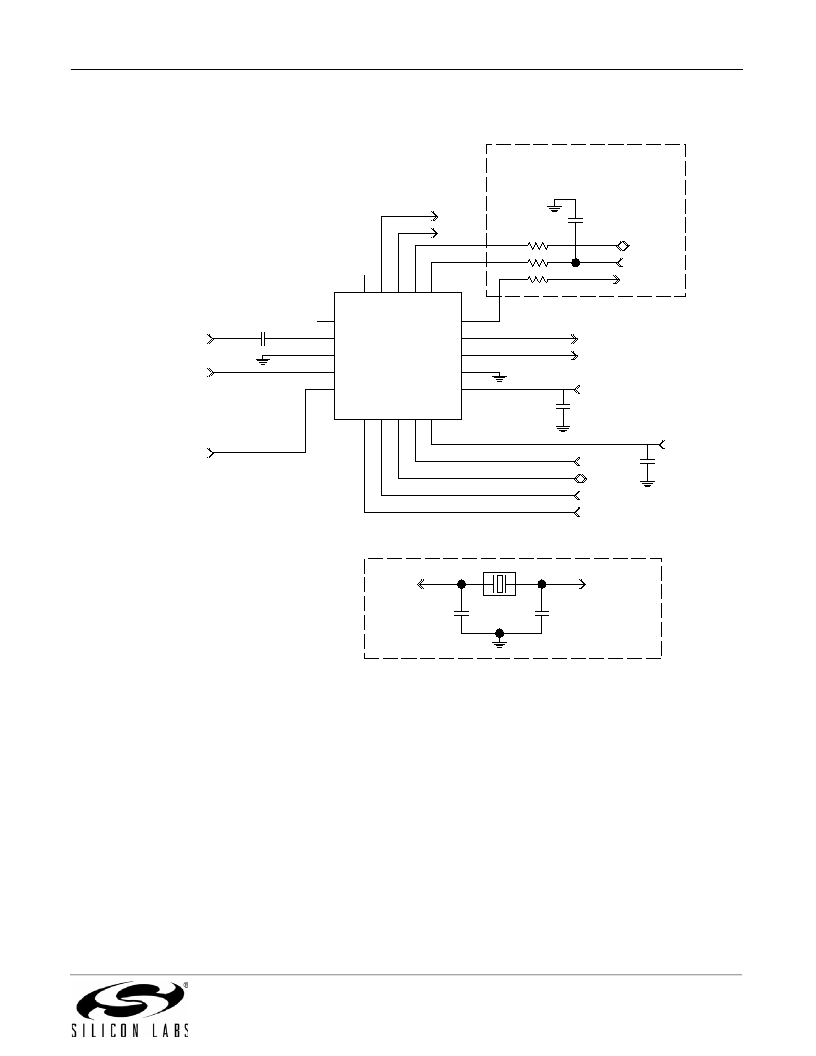
2. Typical Application Schematic
Optional: Digital Audio Out
OPMODE: 0xB0, 0xB5
GPO1
C9
GPO2/INT
R 3
R 2
R 1
GPO3/DCLK
DFS
DOUT
1
NC
DOUT
15
FM Antenna
Embedded Antenna
C2
2
3
4
FMI
RFGND
Si4704/05
LPI
LOUT
ROUT
GND
14
13
12
LOUT
ROUT
5
RSTB
D50
VA
11
2.7 to 5.5 V
C1
VA
1.62 to 3.6 V
RSTB
GPO3
C5
X1
C6
RCLK
SDIO
SCLK
SENB
RCLK
C4
VD
Optional: For Crystal OSC
Notes:
1. Place C1 close to V A pin.
2. Pins 1 and 20 are no connects, leave floating.
3. Place C4 close to DFS pin.
4. To ensure proper operation and receiver performance, follow the guidelines in “AN383: Si47xx Antenna, Schematic,
Layout, and Design Guidelines.” Silicon Laboratories will evaluate schematics and layouts for qualified customers.
5. Pin 2 or Pin 4 connects to the FM antenna interface. Pin 2 is for a half-wave antenna. Pin 4 is for an embedded antenna.
6. Place Si4704/05 as close as possible to antenna jack and keep the FMI and LPI traces as short as possible.
Rev. 1.0
15
发布紧急采购,3分钟左右您将得到回复。
相关PDF资料
SI4706-B20-GM
IC FM RADIO TUNER 20-QFN
SI4712DY-T1-GE3
MOSFET N-CH/SCHOTTKY 30V 8SOIC
SI4731-D50-EVB
BOARD EVAL SI4730/SI4731-D50
SI4731-D50-GM
IC RADIO RECEIVER AM/FM 20-QFN
SI4737-C-EVB
BOARD EVAL SI4737 VERSION C
SI4743-C-EVB
BOARD EVALUATION FOR SI4743-C
SI4770-A-EVB
BOARD EVAL FOR CE AM/FM SI4770
SI4777-A20-GM
IC RCVR AM/FM CE HD-RADIO TUNER
相关代理商/技术参数
SI4706-B10-GM
制造商:Silicon Laboratories Inc 功能描述:
SI4706-B20-GM
功能描述:IC FM RADIO TUNER 20-QFN RoHS:是 类别:RF/IF 和 RFID >> RF 接收器 系列:- 产品培训模块:Lead (SnPb) Finish for COTS 产品变化通告:Product Discontinuation 09/Jan/2012 标准包装:50 系列:* 频率:850MHz ~ 2.175GHz 灵敏度:- 数据传输率 - 最大:- 调制或协议:- 应用:* 电流 - 接收:* 数据接口:PCB,表面贴装 存储容量:- 天线连接器:PCB,表面贴装 特点:- 电源电压:4.75 V ~ 5.25 V 工作温度:0°C ~ 85°C 封装/外壳:40-WFQFN 裸露焊盘 供应商设备封装:40-TQFN-EP(6x6) 包装:托盘
SI4706-B-EVB
功能描述:BOARD EVALUATION FOR SI4706-B RoHS:是 类别:RF/IF 和 RFID >> RF 评估和开发套件,板 系列:- 标准包装:1 系列:- 类型:GPS 接收器 频率:1575MHz 适用于相关产品:- 已供物品:模块 其它名称:SER3796
SI4706-C30-GM
功能描述:IC FM RADIO TUNER 20-QFN RoHS:是 类别:RF/IF 和 RFID >> RF 接收器 系列:- 产品培训模块:Lead (SnPb) Finish for COTS 产品变化通告:Product Discontinuation 09/Jan/2012 标准包装:50 系列:* 频率:850MHz ~ 2.175GHz 灵敏度:- 数据传输率 - 最大:- 调制或协议:- 应用:* 电流 - 接收:* 数据接口:PCB,表面贴装 存储容量:- 天线连接器:PCB,表面贴装 特点:- 电源电压:4.75 V ~ 5.25 V 工作温度:0°C ~ 85°C 封装/外壳:40-WFQFN 裸露焊盘 供应商设备封装:40-TQFN-EP(6x6) 包装:托盘
SI4706-C-EVB
功能描述:BOARD EVALUATION FOR SI4706-C RoHS:是 类别:RF/IF 和 RFID >> RF 评估和开发套件,板 系列:- 标准包装:1 系列:- 类型:GPS 接收器 频率:1575MHz 适用于相关产品:- 已供物品:模块 其它名称:SER3796
SI4706-D50-EVB
功能描述:BOARD EVAL SI4706-D50 20-QFN RoHS:是 类别:RF/IF 和 RFID >> RF 评估和开发套件,板 系列:- 标准包装:1 系列:- 类型:GPS 接收器 频率:1575MHz 适用于相关产品:- 已供物品:模块 其它名称:SER3796
Si4706-D50-GM
功能描述:射频接收器 Adv Hi-perf FM RDS TMC Rcvr Mobile Dev RoHS:否 制造商:Skyworks Solutions, Inc. 类型:GPS Receiver 封装 / 箱体:QFN-24 工作频率:4.092 MHz 工作电源电压:3.3 V 封装:Reel
Si4706-D50-GMR
功能描述:射频接收器 Adv Hi-perf FM RDS TMC Rcvr Mobile Dev RoHS:否 制造商:Skyworks Solutions, Inc. 类型:GPS Receiver 封装 / 箱体:QFN-24 工作频率:4.092 MHz 工作电源电压:3.3 V 封装:Reel
